장비안내
Si BEOL & GaN MPW
- 장비아이디 FS-SM10
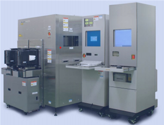
- 장비명 Defect Review Scanning Electron Microscope (결함전자현미경)
- Model RS-4000
- Maker Hitachi
- 담당자 고상현
- 연락처 031-546-6248
- E-Mail sanghyun.ko@kanc.re.kr
- 상 태 ● (가동중)
적용가능한 기판 정보
O (가능) / △ (협의필요) / X (불가능)
| 기판 종류 | 기판 Size | 기판 Type | 기판 두께 | ||||||||||
|---|---|---|---|---|---|---|---|---|---|---|---|---|---|
| Si | III-V | Glass | Flex | 조각 | 2" | 4" | 6" | 8" | 12" | 플랫 | 노치 | Normal | Special |
| O | X | X | X | X | X | X | X | O | X | X | O | O | X |
장비사양(Hardware Specification)
ㆍ Field of View : SEM image 0.7 to 135um square (1,000x to 200,000x)
ㆍ Optical microscope image 0.6mm square(220x), 0.3mm square(440x)
ㆍ Review Throughput : 3.0s/defect or less
ㆍ Specimen Stage : X, Y 0 to 300mm
ㆍ Wafer Loader : 8 inch Open Cassette
ㆍ Electron gun : Schottky emission type
ㆍ Accelerating voltage : 500 to 1,300V variable in increments of 100V, 3kV, 4kV, 5kV, 10kV, 15kV
ㆍ Scanning Modes : S-FAST, FAST, TV, SLOW scan
공정성능(Process Specification)
ㆍ Automatic Defect Review
- Minimum detectable defect size : 0.035 ㎛
- Detection rate : 90% or more
ㆍ Automatic Defect Classification
- Correct classification rate : 85% or more
- Maximum number of categories : 50 categories/recipe
활용분야(Application)
ㆍ 시스템 반도체 공정 중 반도체 웨이퍼 오염입자 측정 및 공정수율 관리를 위한 핵심 검사장비로
불량 분석, 성분 분석 및 조성 분석에 활용한다.
ㆍ 반도체 제조 공정의 결함 검사, 분류, 분석결함의 성분 분석(EDS – Energy Dispersive Spectroscopy)
측정 방법
ㆍ ADR(Automatic Defect Review)
- Wafer Inspection 장비를 통해 감지된 결함/입자 모양을 관찰, 분류, 분석한다.
ㆍ ADC(Automatic Defect Classification)
- Image Server에 Image 정보규칙에 의해 Defect 정보에 따라 자동으로 분류한다.
측정 용도
ㆍ 효율적인 Defect 관리를 통해 발생 Mechanism이나 발생공정을 명확히 규명하여 동일 Defect 발생 원인을 제거한다.
관련 자료
ㆍ Utilities
- Power supply : 200/208/230V AC @ 단상 (60Hz)
- Nitrogen : 400 ~ 880 kPa [gauge pressure]
- Dry air : 600 ~ 880 kPa [gauge pressure]
- Vacuum : 1.3 ~40 kPa [absolute pressure]
ㆍ Environmental Conditions
- Magnetic Field : AC Power, synchronous frequency components: 0.3 uT max.
DC magnetic field fluctuations: 0.1 uT max.
- Vibrations : Frequency: 1Hz ~ 10Hz
- Noise : 75 dB max.
- Humidity : 60% max.
ㆍ Precautions Regarding the Laser Light
| Type | Wavelength | Output | Output class | Application |
|---|---|---|---|---|
| Semiconductor laser | 780nm | 3mW | Class 3B | Wafer alignment |
| He-Ne | 633nm | 1mW | Class 2 | Stage positioning |
| Semiconductor laser | 532nm | 105mW | Class 3B | For darkfield laser (Option) Caution: Wear protection glasses |