장비안내
Si BEOL & GaN MPW
- 장비아이디 FS-PC10
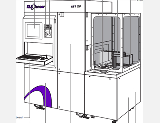
- 장비명 Wafer Defect Inspection System(웨이퍼 결함 검출기)
- Model AIT-XP
- Maker KLA-Tencor
- 담당자 고상현
- 연락처 031-546-6248
- E-Mail sanghyun.ko@kanc.re.kr
- 상 태 ● (가동중)
적용가능한 기판 정보
O (가능) / △ (협의필요) / X (불가능)
| 기판 종류 | 기판 Size | 기판 Type | 기판 두께 | ||||||||||
|---|---|---|---|---|---|---|---|---|---|---|---|---|---|
| Si | III-V | Glass | Flex | 조각 | 2" | 4" | 6" | 8" | 12" | 플랫 | 노치 | Normal | Special |
| O | X | X | X | X | X | X | X | O | X | O | O | O | X |
장비사양(Hardware Specification)
ㆍ Process : Dark Field
ㆍ Fully Integrated Review Microscope (10x, 50x, 100x, 150x objectives)
ㆍ 10um Single Incident Spot Optics
| Spot Size | 10um | 7um | 5um |
|---|---|---|---|
| Bare Silicon | 0.10um | 0.08um | <0.08um |
ㆍ Repeatability
- Bare Wafer < 3% COV (Coefficient of Variation)
- Patterned Wafer: < 3% COV
ㆍ Reproducibility
- Bare Wafer < 3% COV
공정성능(Process Specification)
ㆍ Throughput : 40 Wafers/Hour (@ Spot Size : 10um)
ㆍ Repeatability
- Maker standard wafer : > 90%
- Optical review accuracy on tool : ≤ 4um
- SEM review accuracy : ≤ 5um
ㆍ Alignment : Auto alignment/Manual alignment
ㆍ Image : Patch image / Optic image
ㆍ Edge Exclusion : ≤ 3mm
활용분야(Application)
ㆍ Films
The AIT XP+’s high throughput and sensitivity make it a very cost effective tool for inspecting even rough and grainy deposited films, especially for problems (e.g. voids) at copper deposition before CMP.
ㆍ CMP
The combination of double-darkfield optics, Adaptive Mode technology, and flexible polarization options delivers a high defect capture rate, even on rough, grainy surfaces and in the presence of color variation. Fabs
can detect critical copper CMP-related defects during process monitoring and perform cost effective copper CMP inspection, optimizing the copper interconnect process for maximum yields.
ㆍ Etch
Adaptive Mode and noise reduction benefits of the AIT’s double darkfield architecture increase sensitivity to bridging, shorts, and other critical etch defects, particularly on noisy BEOL layers, making the AIT XP effective for etch monitoring.
ㆍ Photo
The high throughput of the AIT XP makes it a very efficient after developer inspection (ADI) and photo process monitor by allowing production level, full lot inspections aimed at capturing sporadic process issues—key to finding minor problems before they become large, expensive ones.
관련 자료
ㆍ Regulatory Standards (Electrical Directive Compliance)
- Emission : EN 50081-2,EN 55011, Class C
- Immunity : EN 50082-2 , IEC 801-2, Level 4, IEC 801-3, Level 3, IEC 801-4, Level 4
ㆍ Safety / Automation Standards (SEMI and I300I Compliance)
- Safety : S2-93
- Ergonomics : S8-95
- Load/Unload Port: : SEMI E15.1
- Embedded Controller : SECS-II , SEMI E5-91
- Network Connectivity : RS232 and Ethernet TCP/IP
- Reliability : SEMI E10-96
- Other : CE Mark